News update, July 4: Yesterday, Tingbo He, President of Huawei’s Semiconductor Business Division, published the V2 revision of the paper A Time Scaling Theory for Multi-Level Electronic Systems on ChinaXiv, the preprint platform of the Chinese Academy of Sciences. This marks the first major content update to the Tau (τ) Scaling Law since its official debut on May 25, shifting the theory from framework formulation to engineering verification.
Proposed by Huawei, the Tau Scaling Law establishes a new paradigm for semiconductor evolution in the post-Moore’s Law era. Centered on the system time constant τ (signal transmission and response latency) as the unified optimization metric, it replaces traditional geometric scaling with time scaling. Through full-stack collaborative innovations across devices, circuits, chips and entire systems, the law enables continuous improvements in chip performance density and energy efficiency without relying on state-of-the-art lithography processes.
Compared with the initial V1 draft released in May, the V2 edition delivers three pivotal core upgrades as detailed below:
1. Complete Theoretical System Construction
Dispersed arguments from the original manuscript have been consolidated into an organized eight-chapter structure with clearer logical hierarchies. Newly added schematic diagrams and physical cross-section illustrations detail core technologies including the layered τ spacetime model, LogicFolding architecture, bonding interface cross-sections, Unified Bus interconnection framework and Hi-ONE optical engine, rendering the technical roadmap more concrete and traceable.
2. First Release of Mass Production Test Data
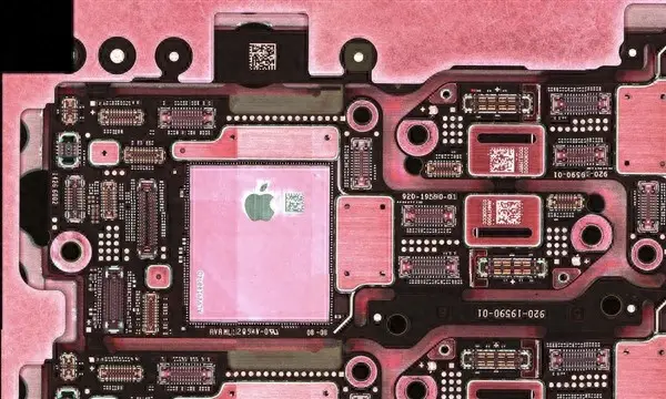
Key measured parameters of the Kirin 2026 chip and its baseline counterpart Kirin 9030 Pro are disclosed, covering operating voltage, working frequency, normalized power consumption, die area and power density. Real-world performance metrics from mass-produced chips validate the practical engineering value of the Tau Scaling Law, filling the V1 version’s gap of heavy theoretical discussion yet insufficient empirical data.
3. Refined Full-Scenario Technical Evolution Roadmap
Clear technical iteration milestones are defined for diverse application scenarios. For mobile terminals, medium- and long-term development paths are supplemented, including relocating TSVs from top metal layers down to the M6 layer and multi-active-layer stacking, laying out actionable phased technical plans.